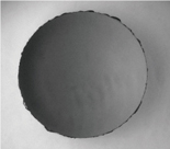
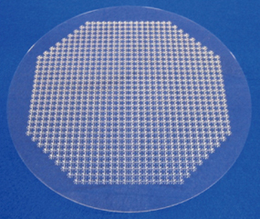
Micro-hole glass
|
Outline
|
 |
|
| Anodic bonding with a silicon wafer can result in solving the out-gas issue. It can be used in the wafer-level-packaging (WLP) process. |
| |
| |
 |
|
|
| |
| |
Features
|
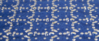
●Micro-hole processing
・min. size φ0.1mm
●Max. glass size φ300 mm
(Some processes are only available up to ø200 mm wafer max.) |
|
Improve bonding yield of device wafers
|
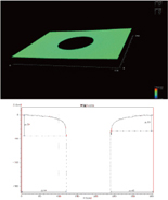
● Suppress sagging around the holes
● Minimize chipping size
・≦10μm is available |
|
|
|
| Standard specifications |
|---|
| Material |
Glass |
| Glass size |
≦φ300mm(*) |
| Min. thickness |
0.15mm |
| Thickness tolerance |
±0.01mm |
| Min. hole size |
φ0.1mm |
| Hole shape |
upon request |
| Hole size tolerance |
±0.02mm |
| Chipping |
≦100μm |
| Cross section shape |
Straight / Taper / Step |
| Metallization process |
Available |
|
Note: These are standard specifications.
In case you have any request except for this, please feel free to contact us. |
|
|
| |
|
|
| |
| |
End user market / Applications
|
| Automotive |
・Pressure sensors, Acceleration sensors.
・Gyroscopes,etc |
|
|
| Semiconductors |
・RF-MEMS switches.
・Image sensors,etc |
|
|
|