Bonding
|
|
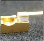
Assembled parts with metal and insulated ceramic by solder
|
It is possible to assemble each part with solder, which is processed by our micro machine processing and metallization.
Solder type: AuSn, AuGe, AgCu etc. |
| |
|
|
|
 |
|
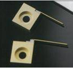
| Mounts/carriers |
|
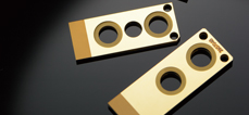
Carriers for optical communication |
|
|
| |
| |
| |
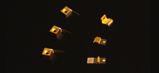
Products processed by this technology
|
|
|
| |
 |
| |
|
|
|
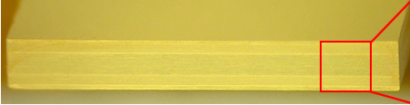 |
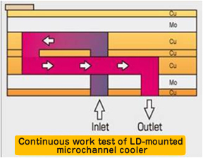
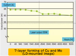
| This product has seven-layer of Cu and Mo which are formed into a 1.6 mm thickness, leading to the control of CTE less than 8 ppm/K. The two technologies below are applied. |
| ・Three-layer forming of central Cu-Mo-Cu by electroforming |
| ・Seven-layer forming into the thickness with the three-layer above, bonded by AuSn solder |
|
|
 |
|
| |
|
|
| |
| With the technologies above, our customized microchannel cooler with LD-mounted on has achieved 5,000 hour endurance time in a continuous work test. |
| |
 |
| |
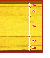
| We have optimized pressure distribution, turbulence kinetic energy distribution, and velocity distribution for our standard products by simulating various microchannels on a design stage. Those can be re-designed according to customers’ needs. |
| |
| |
| |
Products processed by this technology
|
|
|
|
|
|
| |
| |
|
| |
|
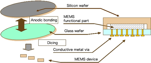
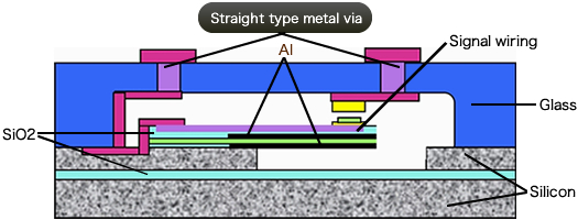
Conductive-through-metal-via processing
|
| This borosilicate glass wafer has a large number of through-conductive-metal-vias, which gives it electrical conductivity. The maximum size of wafer is φ 200 mm. Anodic bonding can be applied to seal a silicon device. |
| |
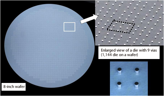 |
| Through glass via(φ0.3mm、10,296 vias) |
| |
 |
| |
 |
| Example applied for RF-MEMS switch |
| |
| |
| |
Products processed by this technology
|
|
|
| |
| |
|
| |
|
|
|
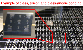
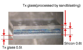
| Anodic bonding is the bonding method where heat and voltage are applied to the borosilicate glass and silicon. It can achieve high-quality bonding because adhesive or solder is not used in the process. |
| |
|
|
| |
 |
| |
|
| |
| |
| |
Products processed by this technology
|
|
|
| |
| |
| |
 |
| |